|
|
| New clean and effective etching method improve laser-induced damage properties |
 |
Text Size: A A A |
|
Antireflection (AR) coatings, which can improve the transmittance of optics and reduce light reflection, are widely used in optics and other optical devices, such as lens, mirrors, optical windows, planar displays, glasses and solar cell modules. Laser damage is more serious in shot wavelength (ultraviolet, UV), especially in space environment. Therefore, more attention is being paid to UV wavelength for multi-wavelength AR coatings.
With dual ion beam sputtering (DIBS) method, AR coatings are dense, stable and they have good binding force of layers. However, the laser damage limits the application of AR coatings in high power laser system or long lifetime laser system. Generally, laser damage of AR coatings is related to the substrate.
Recently, researchers from Shanghai Institute of Optics and Fine Mechanics, Chinese Academy of Sciences, have made systematic study on how different substrate processing methods influence laser induced damage threshold (LIDT). The result was published on Optical Materials.
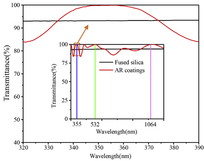
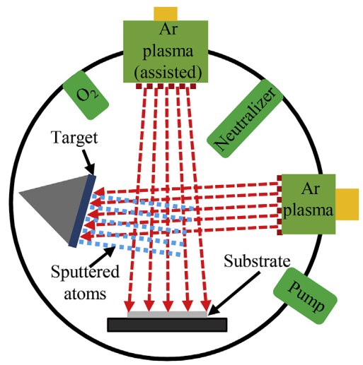
In their experiment, three different cleaning methods (ultrasonic, chemical etching, and plasma etching) were carried to study the laser-induced damage of AR coatings at 355 nm. Transmittance spectrum of the AR coatings and fused silica is shown in Fig. 1. In coating machine of DIBS (VEECO Corp., shown in Fig. 2), the substrates are etching by using assisted ion source. With this plasma method, the coatings could be deposited on the substrates immediately without any movement, which avoided being polluted again in movement or in air.
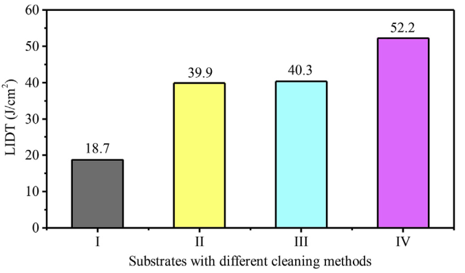
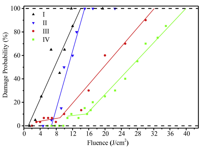
Laser damage threshold of fused silica substrates shows that the argon plasma etching is highly efficient and shows high LIDT, as shown in Fig. 3. Ion beam etching about 200 nm gets the best laser damage properties among the four groups, as shown in Fig. 4. Ion beam etching declines the low LIDT defects drastically and removes plenty of the impurity elements (Ce, Fe, K, and Na). Roughness test shows that the AR coatings (0.704 nm) and substrates (0.623 nm) with ion beam etching are very flat and of low roughness. Ion beam etching reduces the density of deep defect (0.22 mm-2) from substrates greatly compared to ultrasonic (2.20 mm-2) and acid etching (7.92 mm-2).
Moreover, the ultrasonic cleaning method can remove the defects on the substrate with almost no other defects. Chemical etching method will remove both defects on the substrate and the subsurface defects. However, ultrasonic cleaning method has no effect on subsurface defects and it won't totally eliminate the defects on surface. The chemical etching method usually uses solution composed by HF and NH4F, which is named Buffered Oxide Etch (BOE). (NH4F)2SiF6 precipitates are generated after etching. Moreover, after BOE etching, subsurface damage (SSD) is exposed with pits and scratches.
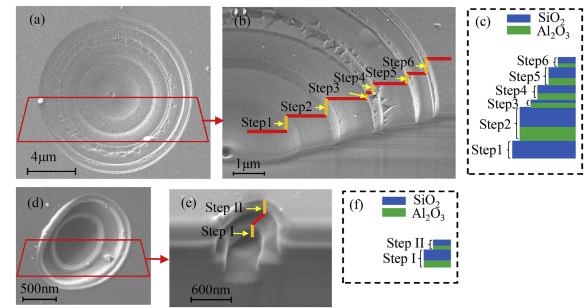
In DIBS AR coatings, two different typical damage morphologies of AR coatings were separated after the ion beam etching method, as shown in Fig. 5 (a) and (d). After ion beam etching, the damage on the coatings was observed close to LIDT, which was attributed to the decline of defects with low LIDT at the substrate.
Damage morphologies show double layers delamination, which can be explained via calculation of layer stress. This study will be helpful for preparation of high LIDT optical coatings.
This work is funded by the NSAF Jointly set up by the National Natural Science Foundation of China and the Chinese Academy of Engineering Physics (No. U1630140), the Youth Innovation Promotion Association, Chinese Academy of Sciences (CAS) (2017289), and the Innovation Foundation of the Chinese Academy of Sciences (1708381X1). Fig. 1. Transmittance spectrum of the AR coatings and fused silica. Fig. 2. Dual ion beam sputtering device schematic. Fig. 3. Laser damage threshold of fused silica substrates with different substrate cleaning methods. Fig. 4. Damage probability of AR coatings by different substrate cleaning methods. Fig. 5. The surface morphology and cross section view of two typical damage pits of AR coatings. Article website: https://doi.org/10.1016/j.optmat.2019.02.034 Contact: Mr. Cao Yong General Administrative Office Shanghai Institute of Optics and Fine Mechanics, CAS |
|
|