β-Ga2O3 is recognized as ultra-wide bandgap semiconductor with a band gap of 4.8–4.9 eV. It has been widely used in metal semiconductor field-effect transistors, metal-oxide-semiconductor field-effect transistors and Schottky barrier diodes devices. Therefore, electrical property is one of the most important ones to optimize device performance.
However, until now, there are only few methods (doping element) to increase the carrier concentration, which is mainly concentrated on Si and Sn. It is difficult to achieve a high doping concentration with Si as a dopant, usually not over 0.2mol%. Moreover, SnO2 and Ge evaporate easily at high temperature, so it is not easy to obtain high-quality and high-doping-concentration Sn/Ge doped β-Ga2O3 single crystals by melt methods.
The research team led by Key Laboratory of Materials for High Power Lasers, Shanghai Institute of Optics and Fine Mechanics and National Lab for Infrared Physics, School of Material Science and Engineering, Shanghai University, has achieved the control of wide range of carrier concentrations of β-Ga2O3 single crystals by Ta5+ doping.
In their experiment, Ta-doped β-Ga2O3 single crystals were grown to regulate the electrical properties of β-Ga2O3. The carrier concentration is intentionally controllable, and can be defined from 3.6×1016 cm-3 to 3.0×1019 cm-3 by controlling Ta concentration. The optical transmittance of Ta-doped single crystals was as high as 70%-80% in the visible region.
In addition, The optical transmittance was distinguished by a decline trend in the IR region, which attributed to the increase of the carrier concentration with Ta doping. Raman spectra revealed that the intensity and the FWHM of GaO6 octahedra peaks rose with increasing Ta content. Meanwhile, in view of nearly the same ionic radii of Ga3+ (0.062 nm) and Ta5+ (0.064 nm), Ta doesn't cause large lattice size changes of β-Ga2O3.
These works pose an effective way to achieve high carrier concentration of β-Ga2O3 single crystal, and by Ta doping, carrier concentration of β-Ga2O3 bulk single crystal can exceed the maximum reported.
The results, entitled “Tuning electrical Conductivity of β-Ga2O3 Single Crystals by Ta doping” were published in Journal of alloys and compounds.
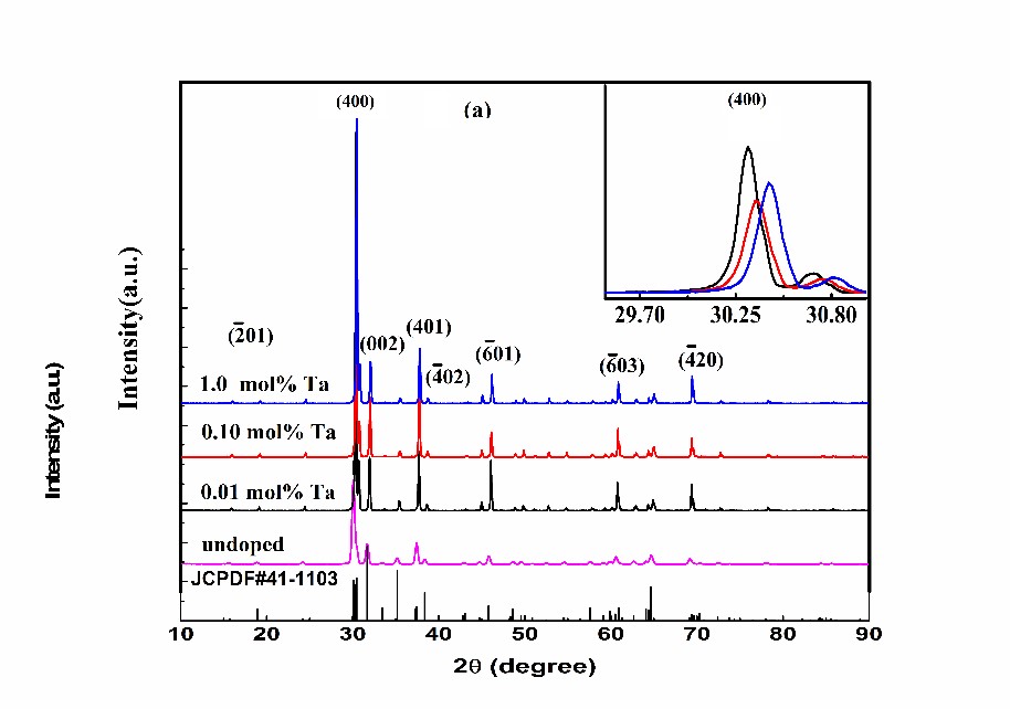
Room-temperature XRD patterns for β-Ga2O3: Ta samples. The inset shows the variation of peak shape with doping for the most intense peak. (Image by SIOM)
Article website: https://www.sciencedirect.com/science/article/pii/S092583881930516X?dgcid=coauthor
Contact:
Mr. Cao Yong
General Administrative Office
Shanghai Institute of Optics and Fine Mechanics, CAS
Email: caoyong@siom.ac.cn
cm-3
