Transition metal dichalcogenides(TMDs) have found applications in high-speed, low-power field-effect transistors (FETs), phototransistors, logic circuits, and so on. While TMDs have been extensively investigated, main group metal monochalcogenides, such as InSe, SnSe, and so on are also under the spot light.
Bulk SnSe was recently found to have a record high thermoelectric figure of merit, and few-layer SnSe was predicted to be a promising 2D material. On the other hand, group IVA dichalcogenides, such as SnSe2, have just started to attract attention.
Despite these efforts in utilizing SnSe2, however, most of its basic electronic properties as a 2D material still remain to be explored.
Researchers at Shanghai Institute of Optics and Fines Mechanics (SIOM) of Chinese Academy of Sciences have investigated the transport properties of few-layer SnSe2 flakes exfoliated from bulk single crystals.
They fabricate n-type FETs with heavily doped few-layer SnSe2, which shows the highest on-off ratio up to -105 at 78 K. Using four-probe measurement, they obtain intrinsic field-effect mobility, with the highest value up to 85 cm2V-1 s-1 at room temperature. Due to the small energy gap between CBM and EF, a seemingly metallic behavior occurs in semiconducting SnSe2. The mobility of SnSe2 FET increases significantly with lowering temperature, suggesting phonon scattering as the main factor limiting its mobility.
The related results were published in Applied Physics Letters
(http://aip.scitation.org/doi/full/10.1063/1.4967744)
Currently they are working on growing higher quality crystals with less dopant concentration. With this improvement, they expect few- to mono-layer SnSe2 FETs to fully demonstrate its great potential as a high-mobility material for applications in nanoelectronic devices.
This work was supported by National Natural Science Foundation of China Science and Technology Commission of Shanghai Municipality and ShanghaiTech University. The nanofabrication facility was supported by the Strategic Priority Research Program (B) of the Chinese Academy of Sciences.
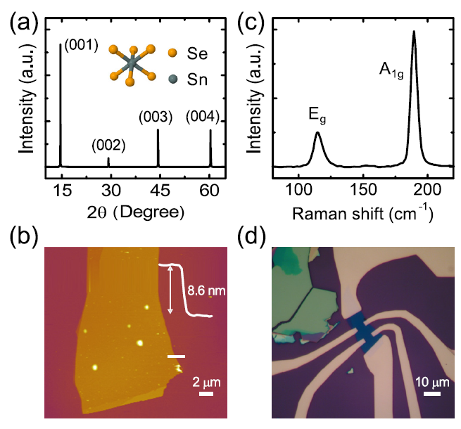
FIG. 1. (a) XRD data of an as-grown SnSe2 crystal. Only peaks corresponding to {001} planes are visible due to the highly oriented van der Waals structure. (b) AFM image of an 8.6 nm thick SnSe2 flake. (c) Raman spectrum of the same sample in (b). (d) Optical microscope image of the 8.6 nm SnSe2 FET device on 300nm silicon dioxide substrate. (Image by Guo Chenglei)
