Liquid crystal (LC) based adaptive optics are used for information processing, optical interconnections, integrated optics, and optical communications due to their tunable optical properties. These properties include LC variable retarders, LC gratings, and LC spatial light modulators. Uniform alignment of the LC is crucial during device fabrication. Numerous methods have been investigated in order to create effective alignment techniques.
A team of researchers from Shanghai Institute of Optics and Fine Mechanics of the Chinese Academy of Sciences (CAS) conducted an experiment to compare the optical, morphological, and laser-induced damage characteristics of rubbed polyimide (PI), SiO2 thin films by glancing angle deposition, and the corresponding LC retarders. The team found that the LC retarder with silicon oxide as an alignment layer had better laser damage resistance. The results of this study were published in Modern Physics Letters B.
A box-type vacuum coating machine (model ZZ550) was used to deposit SiO2 thin films. And SiO2 thin films were deposited at a deposition angle of θ=45°. The surface morphologies of the thin films as observed by atomic force microscopy are shown in Fig. 1. The RMS roughness of SiO2 and PI thin films is 1.059 nm and 1.849 nm, respectively.
The LC retarders were fabricated with a 3-μm cell gap spacer and filled with E7 liquid crystal. The effective dimensions of the LC retarders were 25 mm×30 mm. As shown in Fig. 2, they were checked using crossed polarizers with white-light LED backlights. The laser-induced damage thresholds (LIDTs) of the LC retarder were fitted to 1.84 and 1.45 J/cm2, respectively. The LIDT of the LC retarder using the SiO2 thin film was about 27% higher than that of the LC retarder with the PI film as the alignment layer.
This work was supported by the National Natural Science Foundation of China.
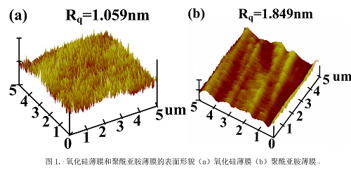
Fig. 1. AFM surface morphology and RMS roughness of SiO2 and PI thin films. (Image by SIOM)

Fig. 2. LCVR viewed through crossed polarizers with white light LED backlight: (a) SiO2 thin film as alignment layer, (b) PI thin film as alignment layer. (Image by SIOM)
Home | About SIOM | Newsroom | International | Admissions | Publications | Contact
@ Shanghai Institute of Optics and Fine Mechanics Tel:02169918000 沪ICP备05015387号-1 Technical support:Qingyun Software