A research team from Shanghai Institute of Optics and Fine Mechanics (SIOM) of the Chinese Academy of Sciences (CAS) demonstrates a robust low-loss optical interface for passive and active lithium niobate photonics. The results were published in Laser & Photonics Reviews on January 22, 2023, and selected to be featured on a frontispiece in the issue.
Single crystalline lithium niobate (LN) is an attractive photonic material owing to its wide transparent window, moderately high refractive index, as well as large acousto-optic, nonlinear, and electro-optic coefficients. Turning the bulk LN crystal into thin film lithium niobate (TFLN) has further enabled the fabrication of high-performance integrated photonic devices for both classical and quantum applications. To realize integrated active photonic devices, TFLN doped with rare earth ions (REI) has recently been employed to demonstrate micro-lasers, waveguide amplifiers, quantum emitters, and quantum memories. Nevertheless, monolithic integration of the active devices fabricated on the REI-doped TFLN with passive TFLN photonic devices has not been demonstrated due to the challenging difficulties in achieving high precision alignment, low-loss interfacing, and reliable bonding.
They demonstrate a robust low-loss optical interface for monolithic integration of passive and active TFLN photonics by tiling the undoped and REI-doped TFLN substrates followed by a single continuous photolithography fabrication process. They achieve a coupling loss of 0.26 dB at the waveguide interface. Furthermore, a four-channel waveguide amplifier array is fabricated, showing a net gain of ~5 dB at 1550-nm wavelength and ~8 dB at 1530-nm wavelength in each REI doped waveguide, respectively.
The strategy of tiling passive and active TFLN substrates to form low-loss optical interfaces for the monolithic integration of passive and active TFLN photonics offers advantages in its high scalability, high reliability, high production rate, and cost-effectiveness.
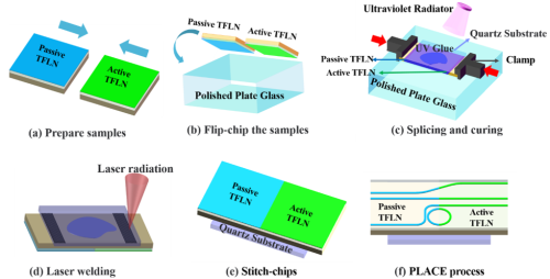
Fig. 1. Schematic of the fabrication process for robust low-loss optical interface of passive and active lithium niobate photonics. (Image by SIOM)
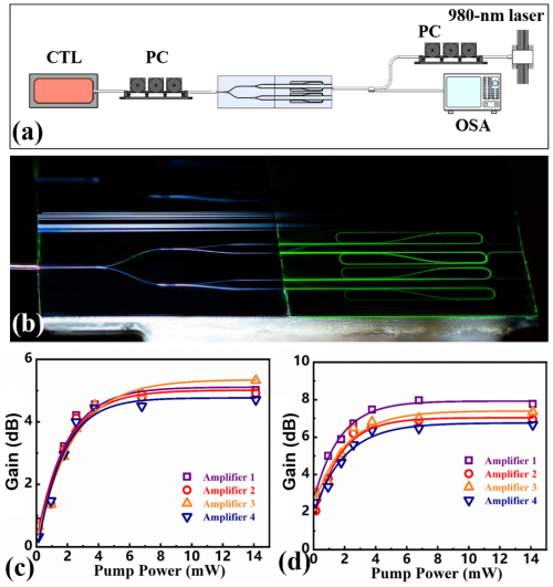
Fig. 2. (a)Experimental setup for the gain measurements on the the four-channel waveguide amplifiers array (CTL: continuously tunable laser; PC: polarization controller; WDM: wavelength division multiplexers; OSA: optical spectrum analyzer). (b) Photo of four-channel waveguide amplifiers array when pumped by 980-nm diode laser. Gain characterization of the four Er3+-doped LN waveguides array for signal wavelengths of (c) 1550 nm and (d) 1530 nm. (Image by SIOM)
Article website:
https://doi.org/10.1002/lpor.202200686
Contact:
WU Xiufeng
General Administrative Office
Shanghai Institute of Optics and Fine Mechanics, CAS
Email: xfwu@siom.ac.cn
Web: http://english.siom.cas.cn/
Home | About SIOM | Newsroom | International | Admissions | Publications | Contact
@ Shanghai Institute of Optics and Fine Mechanics Tel:02169918000 沪ICP备05015387号-1 Technical support:Qingyun Software