A research group from the Shanghai Institute of Optics and Fine Mechanics (SIOM) of the Chinese Academy of Sciences (CAS) has made progress in the printable organic-inorganic hybrid thin-film photodetectors based on one-dimensional (1D) WS2 nanotubes (WS2-NTs) and zero-dimensional (0D) WS2 nanofullerene (WS2-FLs) hybrid with poly(N-vinyl carbazole) (PVK). The research paper has been published in ACS Applied Materials & Interfaces on September 13, 2022.
Photodetectors are the core functional optoelectronic devices and have broad applications in many areas, such as communications, optical sensors, imaging and biomedical devices. By using novel materials or constructing new device structures, self-powered photodetectors can be realized. Printable organic-inorganic hybrid photodetectors have attracted increased interest due to their exceptional properties, such as flexibility, transparency, and low cost for many promising applications. Low-dimensional tungsten disulfide (WS2) nanostructures have outstanding electrical and optical properties, making them ideal candidates for ultrasensitive photodetector devices.
In this research, a novel class of self-powered photodetector was fabricated with hybrid thin films containing two different WS2 nanomaterials, one-dimensional (1D) WS2 nanotubes (WS2-NTs) and zero-dimensional (0D) WS2 nanofullerene (WS2-FLs) hybrid with PVK. Researchers studied the electrical responses of the devices under visible-light illuminations. Due to the increased light absorption and photogating mechanisms, the hybrid film devices exhibit photovoltaic properties under visible light and excellent broad-spectrum photoresponsivity. The properties of nano hybrid thin films are primarily affected by their nanoscale structures and the interactions between the organic matrix and inorganic materials. WS2 is a promising candidate for optoelectronic devices due to its outstanding properties and low-dimensional nature. The WS2 NTs and WS2-FLs could form PN junction with the PVK, a p-type organic semiconductor material. These photodetectors based on hybrid nanofilms have potential applications in optical sensors, imaging devices, wearable electronics, and intelligent optoelectronic systems. Surface-enhanced Raman scattering (SERS) in the WS2-NTs/PVK thin films was also observed.
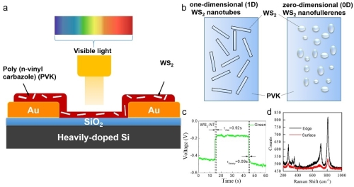
Figure 1. The schematic diagrams of (a) the structure of tungsten disulfide-poly (N-vinyl carbazole) (WS2-PVK) photodetector, (b) the WS2 and PVK hybrid thin films with different morphologies. (c) The photovoltage characteristics of the device, (d) the surface-enhanced Raman scattering (SERS) of the WS2-NTs/PVK hybrid thin film. (Image by SIOM)
Article Website:
https://doi.org/10.1021/acsami.2c10745
Contact:
WU Xiufeng
General Administrative Office
Shanghai Institute of Optics and Fine Mechanics, CAS
Email: xfwu@siom.ac.cn
Web: http://english.siom.cas.cn/
Home | About SIOM | Newsroom | International | Admissions | Publications | Contact
@ Shanghai Institute of Optics and Fine Mechanics Tel:02169918000 沪ICP备05015387号-1 Technical support:Qingyun Software