Recently, researchers from the Shanghai Institute of Optics and Fine Mechanics (SIOM), Chinese Academy of Sciences (CAS) has made new progress in the research of femtosecond laser patterning transparent conductive oxide (TCO) films. They realized the effective regulation of the surface morphology of the film by controlling the fluences of the femtosecond laser, and revealed the law of laser fluence dependence and the formation mechanism of the surface morphology of the film during the process of femtosecond laser patterning. They also proposed a simple and accurate single-pulse laser measurement method for determining femtosecond laser process parameters. Related results were published in the Optics Express on Nov. 3, 2021.
TCO films are widely used in fields such as optical displays, solar cells, and nonlinear optoelectronic devices due to their low cost, excellent photoelectric properties in the visible and large nonlinear optical response in near-infrared region. According to different applications and system designs, patterned TCO films need to be manufactured. Femtosecond laser processing is an important material patterning manufacturing method, and it is a preferred solution to solve non-periodical and special design pattern structures. However, how to control the laser process parameters and obtain a high-contrast pattern boundary is a difficult point in TCO thin film femtosecond laser processing.
The research team systematically studied the evolution law and formation mechanism of the surface pattern of a typical TCO film under the single pulse of femtosecond laser irradiation. The research results show that under the femtosecond laser irradiation, several different types of micro/nano structures appear on the surface of the film and the laser fluence is highly dependent. This laser fluence dependence is attributed to several different removal mechanisms such as surface amorphization, spallation ablation, stress-assisted delamination, boiling evaporation, and phase explosion of the film. Through simulation of the evolution of the hot electrons and lattice temperature in the film over time, it is proved that the femtosecond laser patterning processing of TCO films is essentially a process in which free electrons and bound electrons in the material are stimulated and heated to transfer energy to the lattice. Therefore, controlling the heating of the electrons controls the state of the film after laser processing. Based on this, a simple and accurate method for determining laser process parameters for controlling femtosecond laser processing morphology is proposed.
This work provides a comprehensive analysis of the processing and modification mechanism of femtosecond laser-induced wide-gap semiconductors, and has practical guiding value for the patterned manufacturing of ultrashort laser semiconductor photonic devices.
The research was supported by the National Key Research and Development Program, the National Science and Technology Major Project, the National Natural Science Foundation of China, the Strategic Leading Science and Technology Project of the Chinese Academy of Sciences, and the Special Research Assistant Project of the Chinese Academy of Sciences.
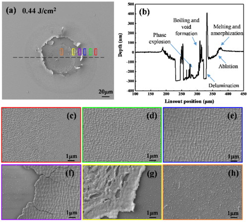
Figure 1. (a) scanning electron microscopy images and (b) surface profles of laser irradiated ITO flm at fluence of 0.44 J/cm2. (c)–(h) Enlarged scanning electron microscopy images where corresponding boxes from (a) are marked. (Image by SIOM)
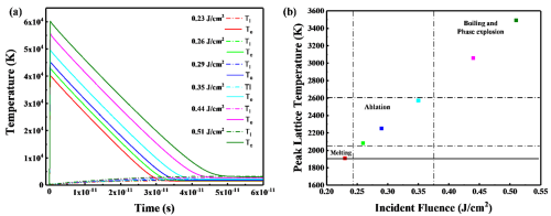
Figure 2. (a) Electron and lattice temperatures after onset of laser irradiation with different laser fluences. (b) Change in peak lattice temperature with diferent applied fluence from 0.23 to 0.55 J/cm2. (Image by SIOM)
Article website:
https://doi.org/10.1364/OE.442882
Contact:
WU Xiufeng
General Administrative Office
Shanghai Institute of Optics and Fine Mechanics, CAS
Email: xfwu@siom.ac.cn
Web: http://english.siom.cas.cn/
Home | About SIOM | Newsroom | International | Admissions | Publications | Contact
@ Shanghai Institute of Optics and Fine Mechanics Tel:02169918000 沪ICP备05015387号-1 Technical support:Qingyun Software