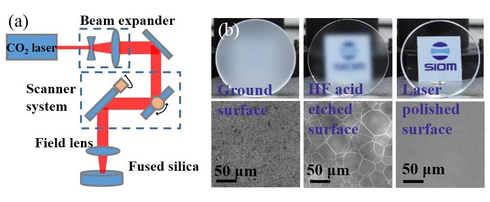
Laser damage in fused silica, particularly ultraviolet laser damage, is still a key problem limiting the development of high-power laser systems. The traditional processing method of fused silica goes through the processes of grinding and chemical mechanical polishing (CMP). This method is time-consuming to achieve an ultra-smooth surface, and is easy to cause surface and sub-surface defects, resulting in a significant reduction in the surface damage threshold of the fused silica.
Recently, the research team of the Shanghai Institute of Optics and Fine Mechanics of the Chinese Academy of Sciences combined chemical etching and CO2 laser polishing to process the ground fused silica. First, chemical etching was used to open the subsurface defects of the ground fused silica. Subsequently, CO2 laser polishing was applied to reduce surface roughness. This combined process not only can efficiently obtain a super-smooth surface with a low surface roughness, but also can improve the damage resistance of fused silica. This work was published in the Optics Letters.
Through damage morphology and a defect analysis, the combined process was shown to avoid the introduction of surface and subsurface defects, including destructive defects, chemical-structure defects, and photoactive mental impurity elements, and obtain fused silica with lower surface defect density, thereby obtaining better damage resistance.
This work was supported by Key Project of the Joint Fund for astronomy of National Natural Science Foundation of China, Outstanding Member of Youth Innovation Promotion Association of Chinese Academy of Sciences and Shanghai Sailing Program.


Contact:
Mr. Wu Xiufeng
General Administrative Office
Shanghai Institute of Optics and Fine Mechanics, CAS
Email: xfwu@siom.ac.cn